


Photolithography in the microelectronics industry
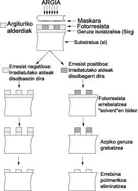
The rapid speed in miniaturization of electronic circuits is a consequence of the manufacturing process technology known as “flat silicon”. With this technology and after taking some steps, complex circuits can be established on silicon discs.
The silicon disc is first covered with a layer of silicon oxide and then with a polymeric material sensitive to photochemical reactions. In general, these materials are resins and are known as the photographic process. A mask is then designed with the appearance of the image to be obtained and, when crossed, the surface of the disc will radiate with ultraviolet or high energy light.
The process of creating a geometry in photopolymers and transferring it to a substrate of another material is called photolithography. This process can be repeated as many times as necessary if you want to build several layers of special geometry on the substrate.
Resins can be positive or negative. In the positive the irradiated aspect becomes soluble and insoluble in the negative. The soluble part is always removed. Resin can be the material that takes the ink or can be used as a mask to record more thoroughly.
The geometry obtained in the polymer is repeated in the insulating layer (silicon oxide) and in the base (silicon) by the development process. Once the resin is removed, the shielding function of silicon oxide causes diffusion doping to occur in periodic table III. Contaminants of groups V and P for obtaining semiconductors type P or N respectively.
The photolithographic technique is used to make thin film resistors. Resistance can be altered, among other factors, by temperature, pressure (piezoresistive effect) or gases. These changes allow for different applications, such as mechanical microsensors and pressure chemicals.
The lithographic process used in the construction of micrometric electronic devices is called microlithography.
The following sections describe a series of parameters and specifications that govern the process of defining a given geometry in a thin layer.
Photolithographic mask manufacturing
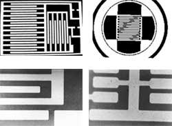
In order to produce a sensitive element of a given geometry, a transparency or a mask template with the same model you want to obtain is needed first. To do this, a model of greater size than the real one is represented and reduced photographically to the necessary size. Working in this way, image defects are reduced and transparency design is more accurate.
The final mask is a type of glass in which the image is defined by an opaque chrome film.
The quality of the transparency used as a template in the lithographic process is measured by transparency or resolution, as well as by the optical density of opaque and transparent aspects. The optical density of the opaque parts of transparency should be high to avoid exposure of the lower photosensitive mask. The edges of the figure must be perfectly defined to allow the direct passage from an optical density to zero and vice versa. Unfortunately, moving from opaque to transparent in reality produces a staggered transition.
Sample preparation
If the fotorresista (resin) is to be retained as best as possible, the sample layer to be retained must undergo special treatments. Polishing, surface cleaning and humidity of less than 45% are required.
Photoresist application technique
With the sample placed in a spinner with adjustable rotation speed, the fotorresists layer is applied. This layer should wet and cover the entire surface.
The characteristic parameters of the centrifuge step are the turning speed, the time and the photoresin/solvent ratio to form a polymeric layer of optimal thickness.
The thicknesses of the photoresisters currently used in the recording of thin film circuits are between the micron and its ten.
After overlapping the polymeric layer, by preheating (“Prebaking”) the solvent remains are steam released to prevent weakening the adhesion to the substrate of the photoresizer.
Exposure to the fotorresist layer
The fotorresist layer substrate will be exposed with ultraviolet light on the device in which it will be in close contact with the photolithographic mask (contact printing) or separated by a small space (projection printing).
Optimal exposure, exposure time, ultraviolet light wavelength and light power are functions, and the final results will show the close relationship between optimal exposure and polymeric layer thickness.
Photosensitive geometries formation process
Especially in the ultraviolet zone there are numerous organic compounds that alter the structure and solubility due to light exposure. The photoresist, in addition to being sensitive to light, must be able to form uniform layers well retained during the recording process, both chemically and physically.
Depending on their responsibility for light, photoresisters can be classified into two. When the surface of the exposed film is more soluble than the unexposed one, a positive image is formed in the developer.
The solubility of the exposed surface can be increased by two types of chemical reactions.
The first of these interrupts the main polymer chain, increasing the molecular weight of the polymer on the sponged surface. Consequently, the solubility in this case is higher than the unexposed surface of higher molecular weight.
The second class modify the exposed surface with polarity compared to the non-exposed. In this way you can also obtain a selective solution of the exposed surface with a suitable developer.
By exposure, when an insoluble image is generated in the developer, a negative image is obtained. Negative images are usually produced by photochemical reactions that cause the lattice of the polymer film. Sareated polymers are totally insoluble in revealing solvent.
Photoresist development and subsequent heating

After development, the sample is obtained by soaking for several seconds in the revealing solvent (solvent) and finishing the process with a distilled water rest bath.
The revealed images are heated (“Postbaking”) to evaporate the solvent residues and thus fully harden the polymer layer, increase chemical stability and improve adhesion to the lower layer.
Recording the bottom layer
Fine layer attack tests are numerous in all types of materials. However, few are published, the rest being secret laboratories. Therefore, until getting a suitable solution, what should be done is try with different special products in different concentrations.
Removal of polymer resin residue
Due to the insolubility of polymer layers, the final removal process is not easy. The degree of difficulty depends on the nature, thickness and substrate of the fotorresistian layer.
The typical procedure is to hot dip effective solvent (stripper). The resin remains are removed through the cleaning process.
Quality of geometries defined in fine films
After mentioning the different steps of the photographic process, it is advisable to analyze the parameters that have been determining in the quality of the obtained element. Thus, the quality of the geometries recorded in fine films depends mainly on the resolution of the polymer mask, the drawing accuracy of the same mask, the time, the temperature, all possible defects of the recording medium, etc., that is, a varied process.
In this complex process there are a number of factors that reduce performance, such as particle pollution and failures in the production process, some without consequences and others catastrophic.
Defective particles can reach the surface of the disc through four main sources: the equipment used in resin processing, chemical compounds, the workplace environment and the same personnel.
Therefore, to prevent these particles from occurring you have to put all possible obstacles, such as special filters, cleaning, cleaning, cleaning of the mouth before entering the work room in case there are cigarette smokers, do not use canes, do not have long beard, etc.
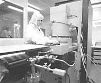
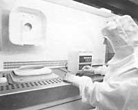
Currently, the minimum characteristics that a clean room should have to be suitable for photolithography are the air filtration system, known in English as HEPA (High Efficiency Particulate Air); control; humidity control and yellow light.
In addition, it is important to place ultra cold water systems, air showers, special breathable soups and adhesives on the floor to clean the shoe sole. On the one hand, it is necessary to take into account that the diameter of a hair is 100 µm and that of a gas residue is 0.5 µm and, on the other, that the size of the images currently obtained is less than that of the micron. Therefore, the harmful effect of particles is immediate.
However, above all these drawbacks, we want to highlight the current and industrial consolidation of the photographic process; in the definition of geography on thin films, photolithography presents the best resolution against any mechanical technique.
Finally, I would like to thank Beñat Odriozola and CEIT Microelectronics Advisor Javier Gracia.
Buletina
Bidali zure helbide elektronikoa eta jaso asteroko buletina zure sarrera-ontzian