


Development of microscopes
The results of the research have had direct consequences for the understanding of science and industrial practice. In this way, the industry has allowed a more precise and profound understanding of traditional materials and a safer, better and cheaper use of them. New types of materials have been developed that offer mechanical and electrical properties that were not even thought of and production control has been improved.
In addition, at a time when Energy and Gross Material is no longer abundant and cheap, the efficient use of these sources is essential.
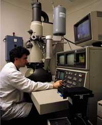
The researcher currently has numerous microscopy techniques. Of them, the Optical Light Microscope, the Electron Scanner Microscope, (S.E.M. ), and Electronic Transmission Microscope (T.E.M.) have been selected here, summarizing its principles, construction and uses or applications.
Going back in history, almost 200 years ago researchers discovered that metals had structure. In 1805 they realized that in England Howard and Germany of Widmänstatt, in the iron meteorites there were limits between different phases.
Indeed. Matter is not continuous and consists of different phases and specimens. It becomes a mistake and, at the same time, an attractive study for science. The core of this science is the saying that best explains and says: “The materials are similar to people: it is their defects that make them interesting.”
After these first observations, Sorby (in Sheffield) already knew the light microscopy technique applied to metal research.
Sorby, discoverer of the close relationship between steel properties and structural defects, gave rise to Metallurgical Science and the technique called Metallography.
Light microscopy was the only technique to study the microstructure in 70 years, until Ruska and others developed the electron microscope in 1930. The maximum increase they could get with light microscopy was a few thousand, as the wavelength of the light no longer supported.
Some elements of the structure of the materials, too small to be analyzed with the optical microscope, caused that in the generation of images, the light radiation was replaced by electron beams. As Quantum Mechanics retains the undulating character of the electron at high speed and estimates that the wavelength is inversely proportional to the wavelength, with reduced wavelengths of up to 0.003 nm associated with high voltage accelerated electrons, the electron microscope can reach enormous magnification and resolution.
At this level, S.E.M. and T.E.M. will be analyzed indicating the advantages and limitations of each other, and pointing out some techniques that combine these microscopes, such as electron diffraction, dispersible energy spectrography, etc.
The enormous advance in microelectronics, computers and vacuum technology has undoubtedly influenced the processing and interpretation of images.
In this spectacular development we cannot fail to mention the Field Microscope of Ions, descendants of T.E.M., the Nobel Prize in 1980, the invention of Binning and Rohre (Microscope of Effect Tunnel Scanner), the Atomic Forces Microscope or the Acoustic Microscope.
Since the description of all of them would be very long, the wording will be limited to those mentioned above.
Optical light microscope
All studies of the microstructure should be initiated at low levels of increase, to be able to visualize the material in general, and for this it would be enough to resort to levels slightly higher than those that the human eye can observe.
Once we are aware of what is seen in these low levels of magnification, we can use more sophisticated microscopes that allow us great increases.
The human eye, without any lens, can see a detail of 0.11 mm (110 microns). By preventing the spaces of the sticks and eye rings, the eye cannot see anything smaller.
Therefore, if we want to see any object smaller than 0.11 mm, we will need the help of the microscope. For example, if we wanted to see a particle of a micron (0.001 mm), we should increase this object to a size of 100 microns that the eye can see. The optical microscope can be used for this purpose.
But the ultimate goal of microscopy is not just to increase the object as many times as desired. It is also intended to achieve maximum resolution, that is, the maximum capacity to differentiate the smallest possible detail.
In the field of optics there are a series of rules that allow to calculate the maximum resolution achievable by any lens. These are:
Resolution g = 0.6 without
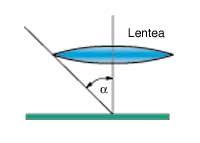
The equation means that the resolution depends on the wavelength of the light and also on the angle called “numerical aperture” (which depends on the angle formed by the deviant rays reaching the lens with the incident beam) (see figure 1).
With this equation it can be calculated that the minimum detail that can differentiate the light microscope is 0.25 microns. In order to visualize the image of this object of 0.25 microns we should multiply it 400 times, since it would create an object of 110 microns that our eye can separate.
The light microscope, relatively simple compared to other instruments mentioned above, is frequently used for the study of microstructures in optical microscopy. In the first steps of Ikerlan, the rapid and correct use of the Optical Microscope allows a first diagnosis of the microstructure. For example, it allows to express the size, shape, quantity, conformity with the microstructure of the composition, the history of the processing, the working conditions and the need for a more specialized technical study.
The basic elements are the Optics and the Lighting System. The study of opaque materials to visible light, which are all metals and many ceramic and polymeric materials, will be limited to the surface and the light microscope should be used as a reflector.
The contrast obtained in the figure arises from the difference of reflection between the different areas that make up the microstructure.
In order to highlight the most important details and defects of the microstructure, it is necessary to prepare the surface of the samples slowly and responsibly to show the true microstructure when analyzing it with the microscope. This means that, if you do not want to get wrong information, it is important to master the sample training technique.
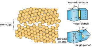
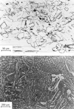
Grain boundaries, for example, are areas of defective surface that form between crystals (or grains) disoriented in polycrystalline materials. In the arrangement of atoms there is a discontinuity between two crystals of different orientation and the atoms that form this interval (grain limit) are in a more energetic (and therefore less stable) state (see figure 2).
Grain boundaries can be seen in the microscope as dark lines. To do this, you must first polish the surface of the sample until it is left at the height of the mirror. The analysis of the thus existing sample is often important for quality control or for the analysis of defects. Microstructural components such as inclusion, intermetallic, fissure and porosity can be analyzed in the polished sample using the Optical Microscope.
Subsequently, in order to visualize the grain limits, the surface is chemically attacked with acidic or basic solution. Due to the unstable state and a more open structure of the aforementioned unit limits, they are the most affected areas. When analyzing the sample with the optical microscope, the incident light will not be reflected as strongly in the grain boundaries, so the grain boundaries will be seen in the microscope as a dark line
However, the Optical Microscope has a problem: you can only focus a plane, you cannot focus any plane that is above or below. Therefore, we will not obtain a three-dimensional image.
Electronic scanner microscope
S.E.M. consists of the following sections:
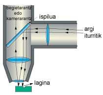
On the one hand, the optical column, which generates electrons, closes the electron beam and scans the same beam across the surface of the sample. On the other hand, the operating table. It controls the focus, the choice of the degree of magnification and the output of photomicrographs of the television screen, among other things
The electron column must be kept empty, because unlike light, electrons are sucked in by air. The electron generator is a cannon or filament of electrons, both wolfram and lantan hexaboruro.
The electron beam, for example in the electronic transmission microscope, fully illuminates the area of the sample of interest. In electronic scanner microscopy, on the contrary, the electron beam accumulates at a very small point and the sample is scanned point by point to obtain the image.
For this purpose, cumulative and stigmatizing lenses are used, obtaining a light point of less than 10 - 5 cm (1,000 Á, 100 nm).
In practice, both the W and LAB 6 filaments allow obtaining 7 nm (70 Eltm) electron points. Keep in mind that, in short, the best resolution will be given by the smallest point of electrons that can be transferred to the sample.
The tension of the electron barrel also increases to the maximum to maximize resolution.
The beam or electrons or point has a horizontal movement along the sample in parallel lines, in which a point of light, such as a cathodic tube or a television screen, performs the same movement simultaneously. The electron beam and the light point perform this scanner with full synchronization throughout the sample.
The signal that sends the material to create the image is collected from each point at which the electron beam explores, measuring the number of electrons emitted by the interaction between the incident electron and matter.
This information passes to the cathodic tube and a spot or spot of bright or dark light appears on the screen depending on the signal change.
If from a point of the material a large number of electrons protrudes, we will see a clear image on the screen. When the number of electrons coming from another area is not so large, we will see on the screen the area of less brightness and, finally, the image that produces an area that barely emits electrons is totally dark.
Electrons that come from outside the sample and are received as a signal after colliding with aggressive electrons are of two types:
- Low energy secondary electrons (less than 10 eV) from the surface layers of the sample ( 50A). The number of electrons collected is dependent on the surface topography and create relief in the image. This is known as topographical contrast.
- Diffuse high energy primary electrons into the sample (0.5 mm). Its tension is equivalent to the aggressive electrons and its number is proportional to the atomic numbers of the chemical elements. Contrast of atomic numbers is obtained.
The two types of electrons are measured in the sample chamber by electron detectors.
As indicated, the variation of point-to-point intensity will result in the last image of the scanned sample surface. In addition, when electrons from all directions are detected, the sample image can be obtained in three dimensions using the Scanner Microscope.
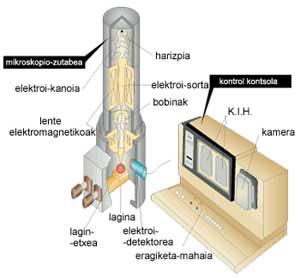
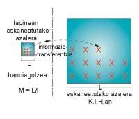
Figure 6 shows how the image or image is generated and how the magnification is controlled.
If the scanned sample surface has a length l and the screen length is L, the resulting image increase is M = L/l. Therefore, if the user has a control of the scanned surface size, increases between 25 and 300000 X can be achieved.
S.E.L. was the first instrument to use the lens free magnification system.
In the following lines we will talk about the use of S.E.M. in Material Research. Applications are many.
As it is said in the historical narrative, S.E.M. has been used in the study of Geological Materials. Also researching Polymers. Latex polymers, also known as emulsion polymers, are colloidal dispersions of polymeric particles in continuous contour. They are widely used in synthetic rubbers, adhesives, latex paints, inks, etc. The average size of the particles in latex is less than 0.1 mm (100 m). Therefore, the S.E.L. has studied the morphology of these particles. its use is usually necessary.
This technique has also found applications in ceramic materials, since the enormous depth of the tool allows studying fractures in small increments.
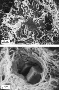
But due to the stability and solidity of metals, these are the most suitable materials for S.E.M. The breakage surfaces are the most studied, being able to determine if the break is ductile or fragile (see figure 7).
Composites are the result of Metal/Ceramics, Polymers/Ceramics or other combinations. Composites are developed to take advantage of the most valuable properties of each of the materials resulting from the combination, being an optimal result. At high temperatures, high strength and ductility materials can be obtained, for example. Also used for the investigation of breakage surfaces. These surfaces are not of any kind, as the mechanical properties of each of the composite components are so different that the break surfaces are very rough and rough.
Finally, it is worth mentioning that 1 in 3 S.E.M. sale is led by semiconductor industry; S.E.M. It is an excellent tool for analyzing semiconductor materials and final products obtained through them.
As a summary you can say: S.E.M., with the same resolution and analytical force as T.E.M., but with ease of use and interpretation of the optical microscope, S.E.M. is one of the most powerful analytical techniques for all types of materials.
On the other hand, when all these images are generated in real time, and being a good control and detection of the sample surface that is intended to be explored, and cooling can be performed.
Using different forms of S.E.M. information can be obtained on the crystallinity of the sample, its orientation and the degree of perfection of the network lens. Finally, the Diffuser Energy Spectrography system also allows chemical microanalysis.
Buletina
Bidali zure helbide elektronikoa eta jaso asteroko buletina zure sarrera-ontzian