

Solar cells in the lab
And from Japan, we come home again. Not so long ago, the research laboratory for photovoltaic cells in the technological part of Zamudio was inaugurated by
a research group of the University of the Basque Country, the Institute of Microelectronic Technology. The mission of the laboratory is to bring the research carried out in the field of photovoltaic cells to the industrial area, which is considered a strategic sector in the future. In order to get to know the work of the research team, we visited the new laboratory in Zamudio.
An investment of two million euros has been made for the construction of the new laboratory of the Institute of Microelectronic Technology. at 1,100 square meters, white rooms and state-of-the-art machines are stacked.
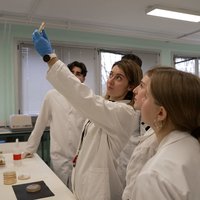
In one of the studies, for example, systems are being developed to measure the quality of the wafers. On the one hand, they make the measurements by means of electroluminescence: they apply voltage to the silicon wafer and analyze the image of the infrared light emitted by it through a camera. With this system, microcracks can be seen on the screen. Measurements are also being made with another system based on photoluminescence.
NEKANE AZKONA; TIM, UPV/EHU: And what we do is excite the cells with light, and then we pick up what it emits in the infrared. It depends on whether this cell is good or not. They do most of what they do so far in this way, take a picture and see where the problems are and where they are not in a cell, where there are cracks and so on. And what we want to do now is to extract from a measurement what is the half-life, a value, not an image, because that is relative, and what we want is to know a specific value.
In Begibista, the faces of the obtains look flat, but they are not. They have a texture made up of micropyramids, a shape that is necessary to absorb sunlight. To make micropyramids, silicon is attacked with various chemical substances. This process is currently very slow and uses a large number of chemical substances. In the laboratory, the time to make micropyramids has been reduced from 40 minutes to 15 minutes and has already been transferred to the
industrial area. VANESSA FANO; TIM, UPV/EHU: We are in contact with a company in Zarautz, Lumiplast, which manufactures printed products. We are developing a machine like this, and if everything goes well, it will cause a great innovation in the market, because nobody has yet managed to extract a machine that performs the texturization in a continuous way. This would be the first.
We are working together with a company from Zarauz, Lumiplast, which is dedicated to the design of machinery to make imprisoned products, we are developing this equipment that if everything goes well will be a great innovation in the market, because no company has followed a team of textures that operate in contact with us. I'm serious about the first machine.
The wafer is inserted from one side of the machine, bathed in various chemicals, and then washed. Thanks to this process, the ability of the wafers to reflect light has been reduced to 10%, which means that they absorb most of the light.
Using the screen printing machine on this side of the laboratory, a metallic layer is applied to the wafers. To date, aluminum has been used in most of the layers, but boron is being used in research.
NEKANE AZKONA; TIM, UPV/EHU: If aluminum is placed on the top, a BSC is obtained and then the profile rises and more electrons can be extracted, but it has two disadvantages. On the one hand, it does not allow the passage of light, and then this difference cannot be used to receive light; and on the other hand, as the cells become thinner and thinner, the cells twist and sometimes break, and again with boron this does not happen, and in addition the cells can be made bifacial. Then they can be placed in a place, such as a place where the ground is, or the ground painted white or, and then we receive light from both sides at once.
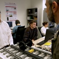
To fix the metal layer, the wafer is inserted into the chain furnace.
In addition to screen printing, they also use the vacuum chamber to create these metal
layers. CRISTINA MONTALBAN; TIM, UPV/EHU: This high vacuum hood is used for deposition of materials, especially metals. Deposition of very thin layers is achieved and under complete control. We managed to control very well the deposition rates on the silicon substrate.
This high vacuum chamber was used to make deposits of materials, principally metals. Very thin, very controlled deposit layers are contemplated. The speed of deposition on silicon substrates is very well controlled.
Lab ovens work between 800 and 1,000 degrees Celsius. Their task is to make the bases of the wafers develop a semiconductor material, usually phosphorus. This is how the solar cells are formed, which allows them to generate electricity when receiving sunlight.
As you can see, the process is slow. The wafers should be introduced and removed from the oven slowly so that they are not damaged by the sudden heating.
In this area the ovens are the present, while the laser is the future.
ALOÑA OTAEGI; TIM, UPV/EHU: We're investigating doping. In fact, in order for the silicon to provide current, it must first be subjected to the introduction of a series of spurities which, for example, require the introduction of phosphorus. What we do then is put the Oblate in this way, we spread a paste and put the Oblate here, on the platform, put it there. So when we put it on the platform, then the platform closes and what we do is act with the laser. The laser is turned on and a beam is seen. What this ray does is soften the paste and also soften the surface of the silicon. Then, when softened, the paste tends to penetrate and the phosphorus diffuses through the silicon. What is achieved in this way is the introduction of these phosphorus spurities. Nowadays in the market or in the industry through ovens, the oven is placed at 800 degrees and at very high temperatures, and what we do here is a cleaner process.
In this laboratory, research on photovoltaic cells is in many situations: from those that are in the beginning to those that are in the patent process.
KENT VARNER; TIM, UPV/EHU: Before I got here, the researchers at the institute had already begun the process of extracting the patent for one of their designs. It is the design of a solar cell with contacts on the back. By this I mean: if you look at this cell, which is a typical solar cell, you see that it has metal stripes, these whitish stripes. The silicon is blue. Then,
on the back, he has other counts, and on one side he has a positive and on the other side he has a negative. We have another design that does not have such contact on the front, as seen in this silicon substrate. And what advantage does it have? It is obvious that these contacts are shadowing. Because of this, the light that is received does not have the ability to pass through the metal and is lost. With these, on the other hand, since there is no metal on the front side, since they are all behind, the efficiency is increased because the entire surface of the wafer can be used.
Before this group arrives, the researchers of the Instituto Nido emptied the transcripts for filing a patent of a suyo design. It's a design of a solar cell that has posterior contacts. What I want you to say with that is if you look at this cell, a conventional solar cell. you see, I've got a few metálicos, this white thing you see. The blue is the silicon.
Luego in the posterior face you see that you have other contacts, and then you are less and more than you are in this other face. But then, we have a design, like we see this silicon substrate, in which there is no such thing as metallic contacts on the front face. and what have you ventured? You can see that those contacts are in the shade. So there's the light that doesn't penetrate the metal, so there's the dead, deficiencies because of it. But in this, they are not metals on the front face, they are all on the posterior face, so that they can assume the effect by providing all the surface of the wafer. At the moment, there is a team of
25 researchers in the laboratory, but it is expected to reach 40. Everyone’s goal is the same: to find ways and systems to make the best use of the sun’s energy.
Buletina
Bidali zure helbide elektronikoa eta jaso asteroko buletina zure sarrera-ontzian