
Smaller than small
2000/06/13 Roa Zubia, Guillermo - Elhuyar Zientzia
This technological society demands less and less technology. There is no more to see the development of computers and phones. With a lot of cost you can buy laptops of two centimeters thick in the market. We are already used to it. However, when analyzing its technological implications, it is really surprising. However, this type of tools does not require minimal technology. Nanotechnology is even smaller.
Opportunity of large companies
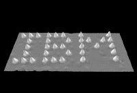
"IBM is making a lot of money to develop nanotechnology," explains Enrike Ortega, a professor at UPV. "I worked at the company's headquarters in New York and we were all investigating it." Recently IBM published its famous experiment. Through atoms he wrote the name of the company, in nanoscopic size. However, it was only a waste to seduce the public. But applications can still be more surprising.
Ortega is a professor of physics at the School of Architecture in San Sebastián, but will carry out his research at the Faculty of Chemistry with the Etxenike team. "We will launch the experimental complement to Etxenike's theoretical research". It is still in works of organization. In fact, the laboratory will be located in another building of the newly opened Donosti International Phisics Center (DIPC). Ortega's colleagues expect the main tool of work: tunnel effect microscopy (STM, Scanning Tunneling Microscope). They are currently waiting for the STM to arrive.
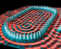
But what is nanotechnology? They are technological structures made in size of atoms and molecules. Therefore, most of the technology that is still used is microtechnology. There are ideas for converting these circuits into nanotechnology, but for the moment very specific and specific applications have been developed. For example, IBM is used punctually on the hard drives of computers. It is difficult. "Microelectronics do little things, but using physics as usual. When you reach the atomic level, quantum physics commands». But that does not imply any inconvenience. The other way around. This has new properties.
It can be said that nanotechnology is in the phase of exploration. However, there is great potential. It should be noted that some apiquias have not been developed since the necessary tools in the manufacturing process remain expensive. But on phones, for example, nanotechnology is already being used. The three main trends are currently the spin valve, the high frequency transsistors (silicio-germanium multisport) and the lasers in solid state.
In the case of the United States there is a free amount of money that has been used in part to invest in the nanotechnology program. Specifically, 500 million dollars have been entered, but this investment will soon double. Expert scientists have drawn up a "panel", a report to show the president. It analyzes the current situation and the future of nanotechnology. As a result of the report, numerous programmes have been launched.

Gai honi buruzko eduki gehiago
Elhuyarrek garatutako teknologia