


The most powerful chip of this century
IBM, Siemens and Toshiba have committed a lot to getting a new chip. Two hundred researchers and a billion dollars are at stake for the superchip to be ready for ten years. It is about reaching the final limit allowed by semiconductor materials, integrating as many transistors as possible into small pieces of silicon. To do this, engineers must renew their integrated circuit manufacturing techniques.
New chip capacity

This new chip can contain 25,000 standard printed pages in your RAM, 30 or 50 times more than conventional PC computers. In RAM the computer contains the information necessary for the immediate treatment and manipulation of users.
As an example, in an image treatment program, the user can use a hundred images on the microcomputer, which currently can only use two. That is, with animated images you can complete up to four seconds, where currently you only have two still photos.
Areas of application
The advances of the new chip will not only apply in the field of animated images. The integration of this new chip will involve a revolution in robotics, vehicles, artificial intelligence, medical engineering, analysis of satellite data in the study of the universe and in other areas of technology.
To realize the progress, let us think that the improvement of microcomputers will be similar to that of large NASA computers. The truth is that the consequences of this chip in the field of applications still cannot be said clearly, because the new applications are still only in the imagination.
Evolution of chips

The first ancestor of this superchip, designed by IBM and its two partners, was created in 1964 by IBM itself. Then the square piece of silicon had only one transistor, but from there the integration of electronic components has grown at full speed. In 1972 they managed to integrate 1,000 transistors into a chip, in 1976 4,000, in 1978 16,000 and currently integrate up to 16 million transistors on the surface of the silicon part.
The aim of this competition to put new brands every day is twofold: one technical and one economic. Technically, the closer the electronic components are, the shorter the connections and the faster the information is transmitted. Also from the economic point of view it is convenient to integrate the largest number of electronic components in the same piece and surface. And it is that machines made with chips with many components at the same power are cheaper than those made with fewer components.
Towards monopoly in the chip world?
In this competition of integration and miniaturization, the bet for the superchi is the way to win the game to the competition. It is about directly overcoming the 64 megabite memory project (the bit is the 0 or 1 signal binary information saved on the transistor). Siemens, IBM and Toshiba want to put a superchip of the same price against the chip of their competitors. With a much more powerful chip at the same price, they can have at their disposal the world computer fair.
In the field of semiconductors there is a well-known law. According to this law, any chip (whatever the power) before or shortly after reaches 10 dollars. The reason is very simple to understand: when a new generation of chips appears, it replaces the previous ones because electronics manufacturers prefer to replace the four slow chips with a fast chip.
It is clear that those who take out the chip of new generation will have in their hands the monopoly and will get a lot of performance. When it is just released, the chip is sold four or five times more expensive than the rest, until the competition goes the same and the prices drop to the ground. Therefore, IBM, Siemens and Toshiba will be able to advance a few years and sell an expensive superchip.
At the risk of competition, ATT, NEC, Fujitsu and AMD come together and expect to reach 256 megabites from the current 64 megabite chip.
Manufacturing conditions
However, for the manufacture of the superchip an investment of one billion dollars has been announced, which will only be for starters. The project will be completed with another two billion. Because the manufacturing conditions are enormous.
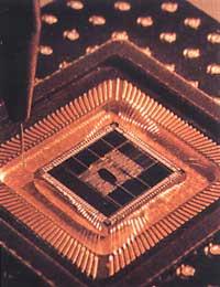
To record circuits in the silicon semiconductor, dust is a great enemy. A drop of millimeter dust is enough to spoil the circuit. Therefore, the most expensive industrial work is undoubtedly the integrated circuit of semiconductors. On the one hand, we have to work in controlled atmosphere rooms, and on the other hand, the production and control machinery, of great precision, is very expensive.
At IBM's workshops around Paris, for example, every year it costs you to upgrade your facility's technology to about twenty billion pesetas (about a billion pounds).
The aspect of the workshops is also very different. It seems more than the assembly chain workshop to shield the room where the safes of the banks are located. It is impossible to access the room where semiconductors are recorded. With special suit and all safety measures (open doors with magnetic card, etc.) Access to these rooms is limited to one or another type of people.
In these rooms it is made vacuum at submicron scale for the application of different substances to semiconductors and for the realization of channels on the silicon surface. A network is placed to deposit the “doping” substances (boron, phosphorus, arsenic,…) in certain places of the material. In some areas electrical conductivity is modified and thus negatively charged electrons are shown which pathways they must traverse.
However, anyone who wants to delve into the manufacture of integrated circuits can use the article called “Integrated Circuits”. Amaia Ibarra and Txelo Ruiz have written and “Elhuyar. Zientzia eta Teknika” in issue 48 of this magazine (June 1991, 23-31). page) was published.
Miniaturization Race
The manufacture of the 256 megabite chip will require more developed techniques than current ones. Before making the first prototype, much more compact circuits must be designed. So far, laboratories that manufacture integrated circuits have taken advantage of the computerized graphical data used in previous generations of chips. For the design of new chips has been reducing the size of electronic components so that information circulates faster. In this way they get a chip of a megabit in 37 square millimeters of silicon. That's only half of what I needed seven years ago.
But for the superchips that want to make IBM, Siemens and Toshiba that size is too big. An obstacle will be the realization of lines of 0.25 microns (the micron is one thousandth of the millimeter). The wavelength of the light beam used for this purpose must also be adequate, since the object with a wavelength greater than the thickness of the line cannot be displayed.
Until the 1980s, with visible wavelength light between 0.4 and 0.8 microns, 2 micron thick lines could be seen on 64 or 256 kilobits chips. Then they had to use ultraviolet rays (wavelength less than 0.4 microns), but in this new 256 megabites they will have to go to x-rays. This way, the wavelength can be reduced to a thousand microns. However, X-rays have an obstacle, as they traverse almost all materials. Therefore, this superchip of 256 megabites must be photolithographed with a band of ultraviolet of small wavelength selected. From there you should avoid the X-ray barrier for the next generations of chips or devise a new manufacturing system.
In any case, it is expected that in the 2010-2020 decade there will be chips of 1 and 4 gigabites (billion bits), from there engineers will not worry about being on the physical border. The 16 gigabit chip would require the installation of very small electronic components in silicon (the hundredth of micron) and could not be operated electrostatically to electrons. Under tension the electrons would reach a temperature of thousands of degrees and sharply destroy the semiconductor.
Buletina
Bidali zure helbide elektronikoa eta jaso asteroko buletina zure sarrera-ontzian