


Grafeno, a new material
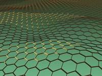
Imagine for a moment the thinnest object of our life. What can it be? With a quick response we can say that it is a sheet of paper or a razor blade. But to reduce to our day to day is much, because outside of it there is a material one hundred thousand times thinner than a sheet of paper, which only has the thickness of an atom. A single atom. Literally, nothing can be thinner than that. This amazing material is graphene, formed by a single layer of carbon atoms with a hexagonal structure in the form of bee cells.
Carbon atoms are components of a large number of materials; the best known are diamond (where atoms form a tetragonal network forming a high value transparent insulator) and graphite (where several layers of cells form an opaque and conductive compound, such as the pain of pencils).
In 2004, André Geim and Konstantin Novoselov, two researchers at the University of Manchester in the UK, discovered that graphite layers could be separated by a simple and economical method: adhesive paper. Once glued and welded the adhesive, they managed to separate the layers of the graphite to obtain a surface of a single layer of atoms settled on a substrate. After extensive experimental tests with microscopy techniques, even the most skeptical recognized the novelty of the material found, the door of a world full of possibilities and perhaps applications was opened.
It was immediately proved that the electrons were moving in this material in a way that had never been observed until then. This behavior was not explained in a conventional way, but by equations extracted directly from the physics of particles of great energy. Suddenly, in addition to finding a new material, the science that describes it was new. Electrons move at high speed in graphene, faster than in other materials. With this feature it seemed that the way was opened to produce faster and lower consumption transistors (base of any electronic device, like the computer).
However, graphene also presents intrinsic problems that limit electronic applications. The band hollow semiconductor ( band gap ) is practically null, which can limit applications in conventional transistors. In addition, we must not forget that silicon, thanks to its excellent chemical and physical properties, has left out of the competition all the competitors that have emerged in the last 50 years, at the same time that the electronics industry has made a huge financial investment in silicon, of which there is an accumulated knowledge for years. For the industry to start using a new material, it is essential to expect good economic performance (and much higher than the previous one).
However, and despite the limits, if we take into account the high speed of the electrons, the graphene could have a certain application pit in high frequency electronics, where other semiconductor materials do not work properly. Some multinationals, like IBM, are studying this line of work and we have already begun to see the first results of this research.
In addition to being shocking by itself the use of graphene for radiofrequency applications, we must not forget that the material is relatively transparent (remember that most metal materials are opaque) and therefore interesting for optical applications. For example, in the solar cells or in the organic light emitting diodes (OLED) that are currently anywhere, it is essential that an electrode allows the passage of light and, at the same time, the electric current. It is difficult for graphene to compete with electrode oxides -- high transparency and very stable -- in optical applications that require great luminosity, such as television screens. However, flexible or portable displays can be the field of application of graphene, due to the union between material transparency and mechanical resistance.
To get some of these ideas full of hope from research laboratories and have a commercial application it is necessary to produce graphene in very high quantities and with quality control. It is clear that an industrial application cannot depend on a material produced by hand and with adhesive tape and that it does not exceed several hundred square micrometers. Fortunately, there are other methods to create high-quality graphene olatas. In particular, the method that consists of deposition from the steam phase has allowed to fix the layers of graphene in several metals, which can reproduce on a larger scale and at a low cost --relativo-. I think that when the method is fully optimized, it will be a source of high quality materials for industrial use.
With those close to graphene, carbon nanotubes and fullerenes, will it happen with graphene? Will it be a material that only interests scientists and does not reach the industry or consumers? Will the Nobel Prize be awarded to researchers six years after the discovery of the adhesive tape phenomenon the upper limit of the glory of graphene?
It's always hard to predict the future, but I think we're facing a material that's going to influence our lives through completely new electronic devices. When important scientific discoveries of this type occur, it tends to blow, but it is possible that in a few years we can see the actual applications of graphene in electronic devices. Beyond that limit, dreaming can be easy, but graphene is so exciting from so many aspects that dreaming of it is inevitable.
Buletina
Bidali zure helbide elektronikoa eta jaso asteroko buletina zure sarrera-ontzian