

Electronic Transmission Microscope
The idea of using electron beams to obtain expanded images was carried out in 1932 by two groups of researchers from Berlin.
In addition to Medicine and Biology, electron microscopy has been used since its inception in Material Research.
Some structural defects until then tested theoretically or indirectly were directly observed with the electron microscope. Since then, although the volume of research conducted with the electron microscope has been enormous at the publication level, the volume of material analyzed with the electron microscope worldwide is only ¼ 1 mm3!
The reason for this fascinating fact lies in the enormous increases that can be obtained from the Electron Microscope. To reach statistically significant conclusions it will be necessary, therefore, to analyze sufficient samples, since the volume of matter is very reduced by each micrograph (microscope photo) (ª ?0.4 m3).
Electronic transmission microscope (T.E.M.) can show the most important features of the microstructure in both amorphous and crystalline materials. The latter uses the phenomenon of electron diffraction to detect the structure and orientation of some characteristic (perhaps 1 ?m in diameter) by diffraction images, or by taking advantage of the same diffraction process to obtain a real contrasted image of dislocations, congestion defects or small precipitates.
Electrons are the elements that form the image in the transmission electron microscope, as in the scanner.
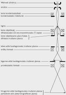
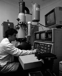
The electron beam is generated at the top of the column located in the gap, once the W or LaB6 filament is heated. The electron beam is accelerated by a potential difference between 75 and 120 kV (or higher) below the column and condensed by an electromagnetic condensing lens up to a minimum diameter of 3 to 5 ?m, then through a section of the sample placed in the applicator (see top of Figure 1). The scanned sample should be very fine for electrons to pass through.
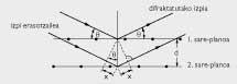
If the object is crystalline, without changing direction, in addition to the primary or transmitted beam that crosses the sample, there are several electrons that disperse coherently in certain angles and directions of Bragg “with Bragg direction”. Electron diffraction has its cause, among other things, in the periodicity or order of the crystalline network, so the study of these diffracted electrons will provide invaluable information about the structure of the material.
Figure 2 shows the atomic ordering of any crystalline structure, being the space between planes “d”. The primary beam, with ? wavelength, affects these planes with angle 9 and the secondary or diffracted beam leaves with angle 29. For diffraction to occur it is therefore necessary to comply with the following law, which is called “Bragg equation”:
n| = 2 sincere
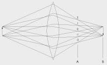
The difference and relationship between the information obtained with the non-imaging diffraction technique (the one that gives the point image) and the one that provides real images can be understood as:
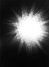
As can be seen in figure 3, each beam of electrons distributed by diffraction generates a point in the focal plane of the lens, specifically in plane A. The image that forms all points is called diffraction image.
If the optical path of the rays is continued, it can be observed that by combining the rays of the different beams of diffracted electrons the image is created in plane B.
The informative content from both the diffraction image and the actual image must be the same (unless between planes A and B an opening is placed that results in a restriction of information, as mentioned below), but distributed differently.
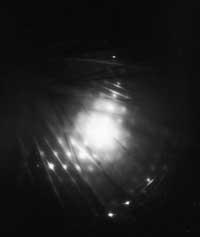
The diffraction figure collects the average information of the total sample. In the actual image the distribution of this information by points is recovered.
In practice, the diffraction imaging technique is used to determine the structure of the crystals and the imaging technique to know in detail the distribution of microstructure characteristics.
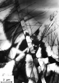
Figure 4 shows the actual image with its corresponding diffraction image. When the image is generated with the beam of electrons not diffracted, that is, with the transmitted ray, we obtain the image of the Clear Field:
According to the orientation to the aggressive ray of the sample, in the defined rights delimited by the angles of Bragg, the electron beams that will be more or less diffracted with the diaphragm or aperture objective (which forms an angle smaller than the diffracted angle) established in the focal plane of the objective lens (where the diffraction image is generated), only the image transmitted by the column can be seen (1). This will allow you to get a more contrasted image.
Using the electron beam that passes through the aperture target, the objective lens creates the first augmented image of the sample. On this same plane is the central opening.
The central lens and projection lenses multiply this first image by two. As in light optics, the total increase is produced by the product of increases produced by different lenses. The last magnified image on three occasions can be seen on fluorescent screen and, if desired, printed on photographic plates.
The wide extension field is obtained with different excitation measures of these central lenses.
This screen will display in black the area of the sample in which the electron has diverted widely because these rays have not let pass the objective openings and, therefore, great intensity of the incident beam has been eliminated. Instead, areas that have not generated diffraction will give a clear contrast.
This type of contrast obtained in the figure is known as “diffraction contrast” or “orientation contrast” and, therefore, is generated with different deviations or diffraction of electrons that are derived from both the elements of the microstructure and the defects.
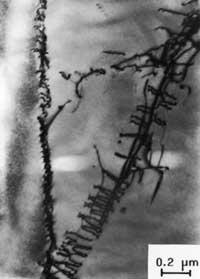
Dislocations, for example (which are defects of the microstructure), which have a nonlinear (defective) arrangement of atoms, strongly repel electrons from their attack direction, so we will see them as dark lines on the microscope screen (see figure 5).
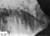
As indicated, for electrons to pass through the sample it is necessary that the area in question be very thin, that is, transparent to electrons. The ideal thickness ranges from 100Á to micro.
Therefore, the sample foils of 3 mm diameter are prepared and in the first preparatory step it thins up to 100 ?m, obtaining a thickness of ª 1 ?m both by electrolytic polishing and by attack of the ion beam. The result is a small perforated disco with several very thin areas around the hole. These are the main areas of microscope study.
The greatest contribution of the T.E.M. is to highlight the crystallographic defects presented by solids. Consequently, the properties and behavior of these errors have been analyzed in detail and the conclusions of these observations have been very useful in the science of materials.
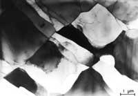
Figure 6 shows another photograph of Aisi 304 stainless steel in T.E.M. with its diffraction image.
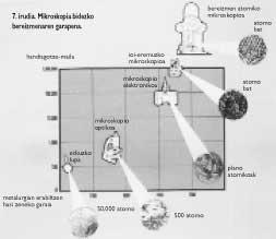
Figure 7 shows the comparison of extensions and resolutions obtained through the three techniques mentioned.
Buletina
Bidali zure helbide elektronikoa eta jaso asteroko buletina zure sarrera-ontzian